I've been messing with an AD9850 DDS Board, on and off, for a while now. Initially I thought I'd just be able to replicate some one else's project, like the following ones from
Instructables:
But, for various reasons I couldn't get things to work how I wanted them to. I also looked at different Arduino Libraries for the AD9850 and had problems understanding the different functions in the libraries and how to call them, etc. (primarily due to my beginner/noob skills in programming). As a result,I decided to take a step back and go to a more basic and direct level and not use a Library but instead just write more direct code.
My first step is to
really dig into the datasheet for the
AD9850 - (this is the datasheet for the chip from
Analog Devices).
Important Info from datasheet:
- PSU to chip/board is 5V
- logic levels are also 5V
- Important Pins: (descriptions on p5 of the datasheet)
- Vcc
- GND
- D7 - this is our serial data input pin
- W-CLK - Word Load Clock (our clock pin for loading serial data) - when pulled high it loads next bit into register then pull low before starting over with next bit
- FQUP - Frequency Update Pin (like a latch pin for a shift register) - pulled high then low to enable serial mode and again after filling register to load bits in to update frequency (not completely clear in datasheet)
- RESET - Master Reset for board and registers on board (need to perform at start and possibly before each time frequency is updated/changed)
The Serial Enable and Load sequence is on p12 of the datasheet. Another important detail is the timing diagrams on p11 (list the minimum times between clock pulses, etc as well as the minimal pulse width's).
To set the frequency of the AD9850 we need to load a 40 bit word through the D7(serial data loading pin). This is summarized on page 9 of the datasheet: 32 bits set the frequency, 3 bits for control and power down, 5 bits for the phase shift of the frequency. Page's 12 and 13 give better information on the sequences for powering on the chip, resetting the registers, loading the registers and powering off the chip. Bits 32, 33 and 34 should all be set to 0 (binary) to avoid powering down chip or enabling factory test modes.
I will post a clearer run down on addressing this chip/board serially (bit order, timing sequence, etc.) once I get back to my workbench to actually test everything.
A quick note: the AD9850 DDS board I am using I ordered on
ebay from
NYPlatform (that's the link to the store, since they change their listings regularly). A labeled picture of the board as well as the board schematic are below:
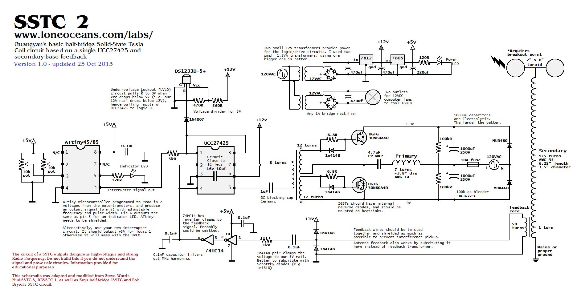
My primary motivation for getting back to this particular project is to enable me to further test my new SSTC2 and verifying everything concerning it before First Light.
Back to
Project Signal Generator